
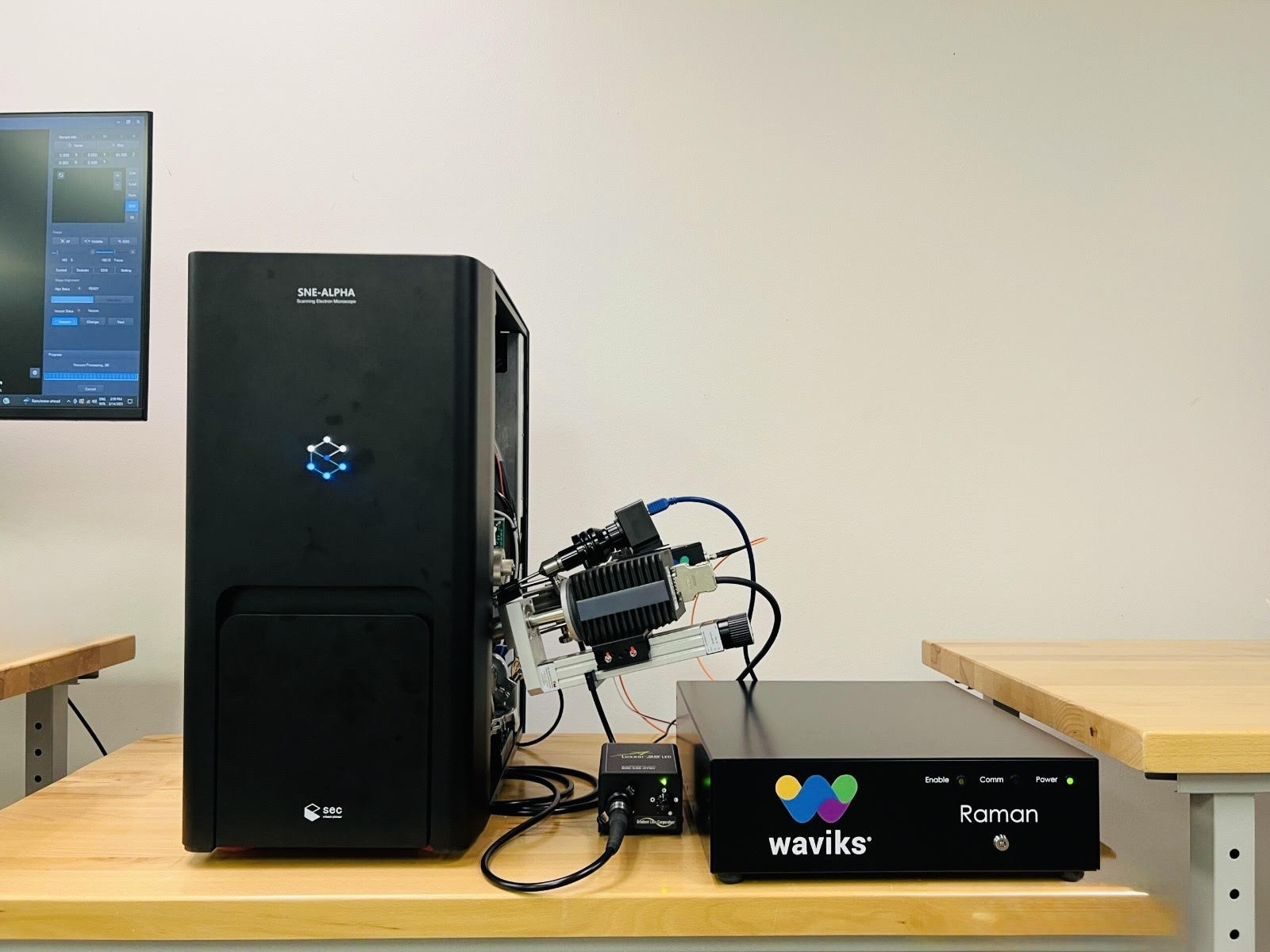
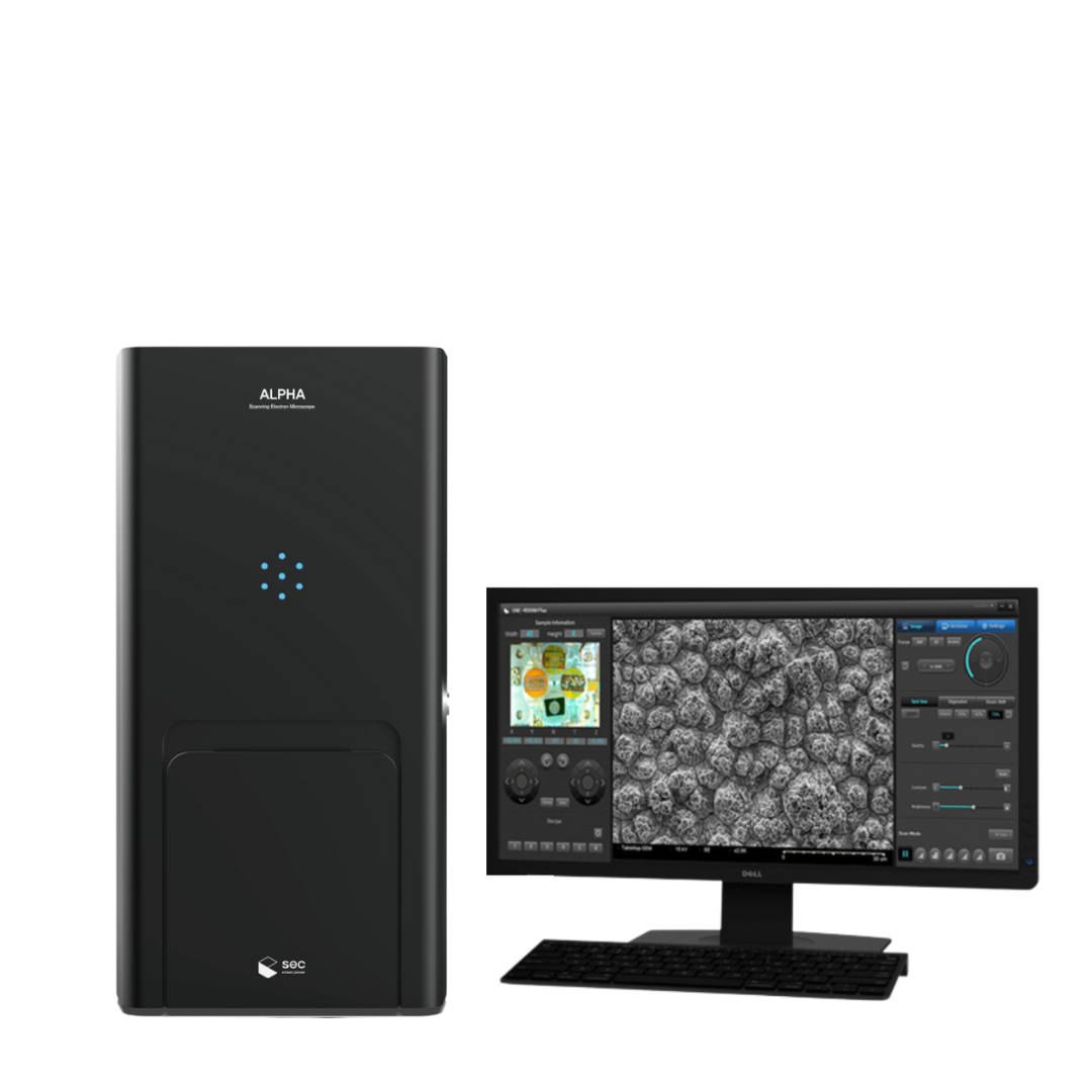
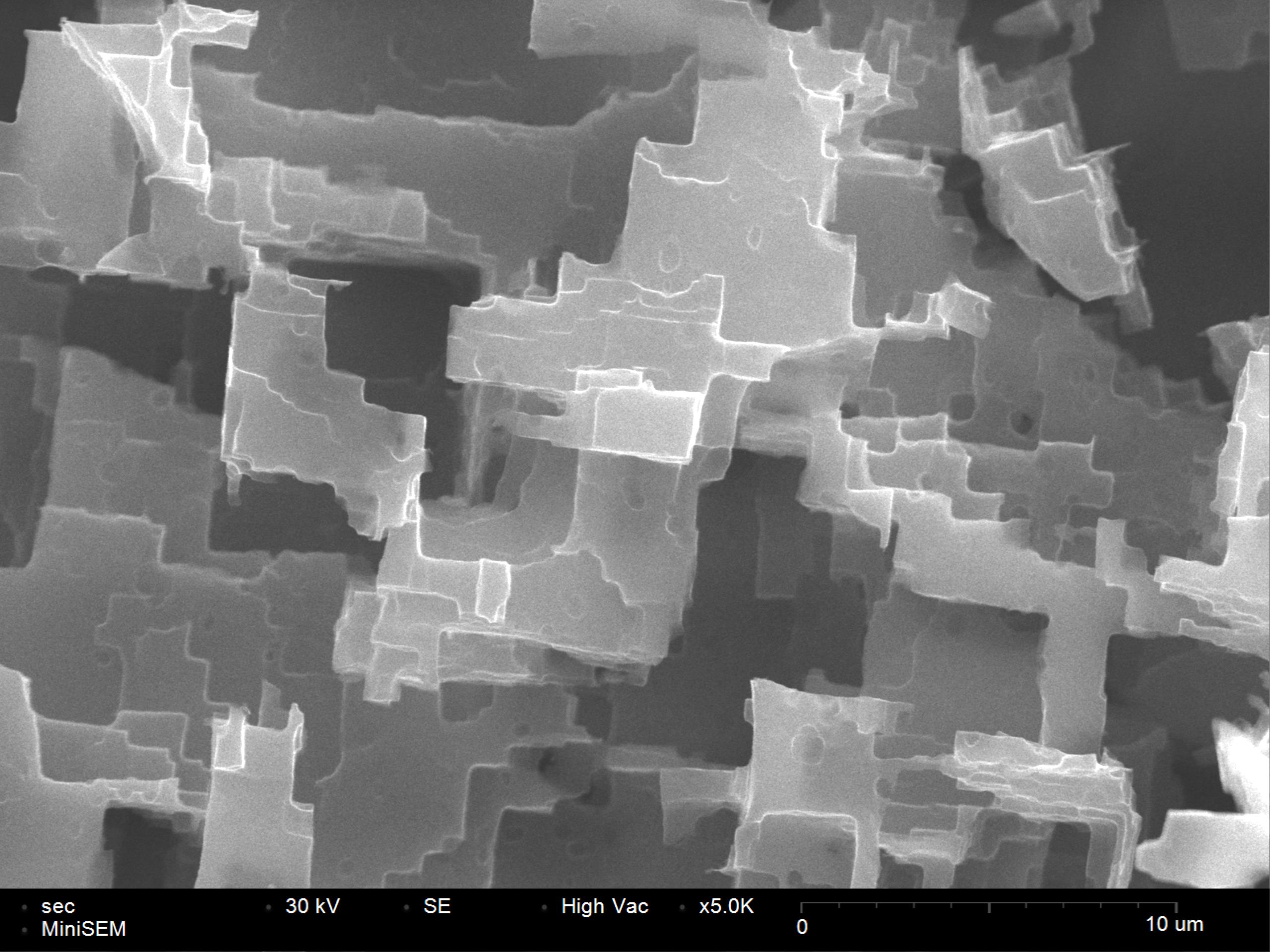
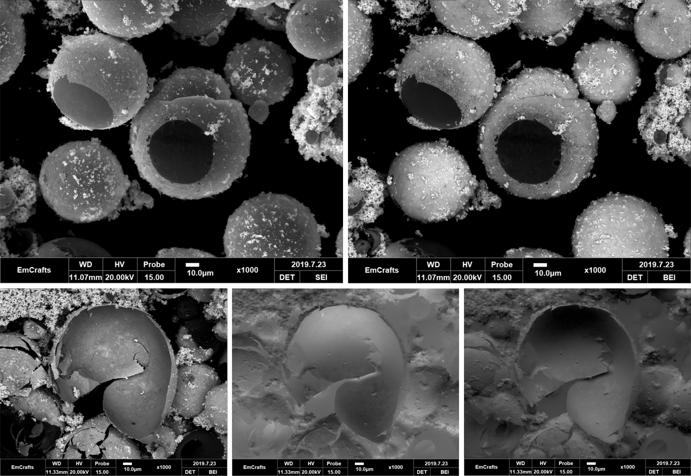
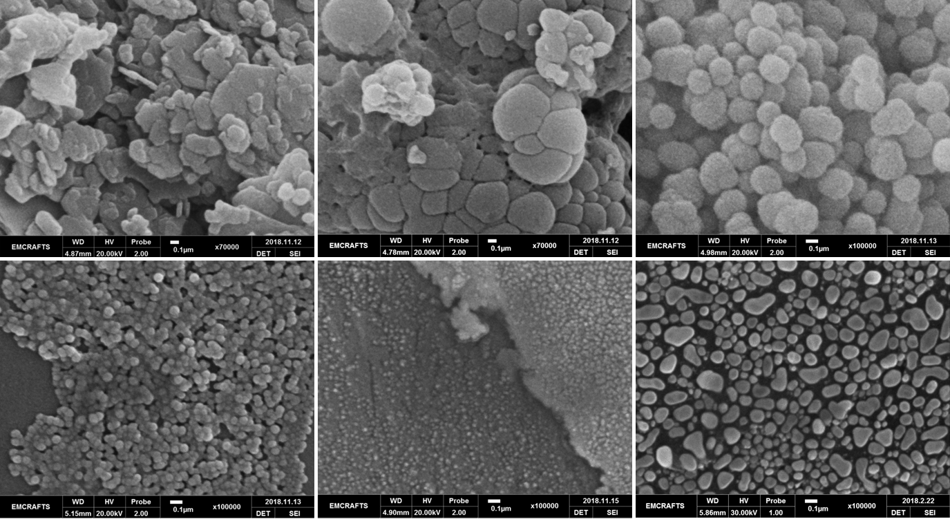
Scanning Electron Microscope

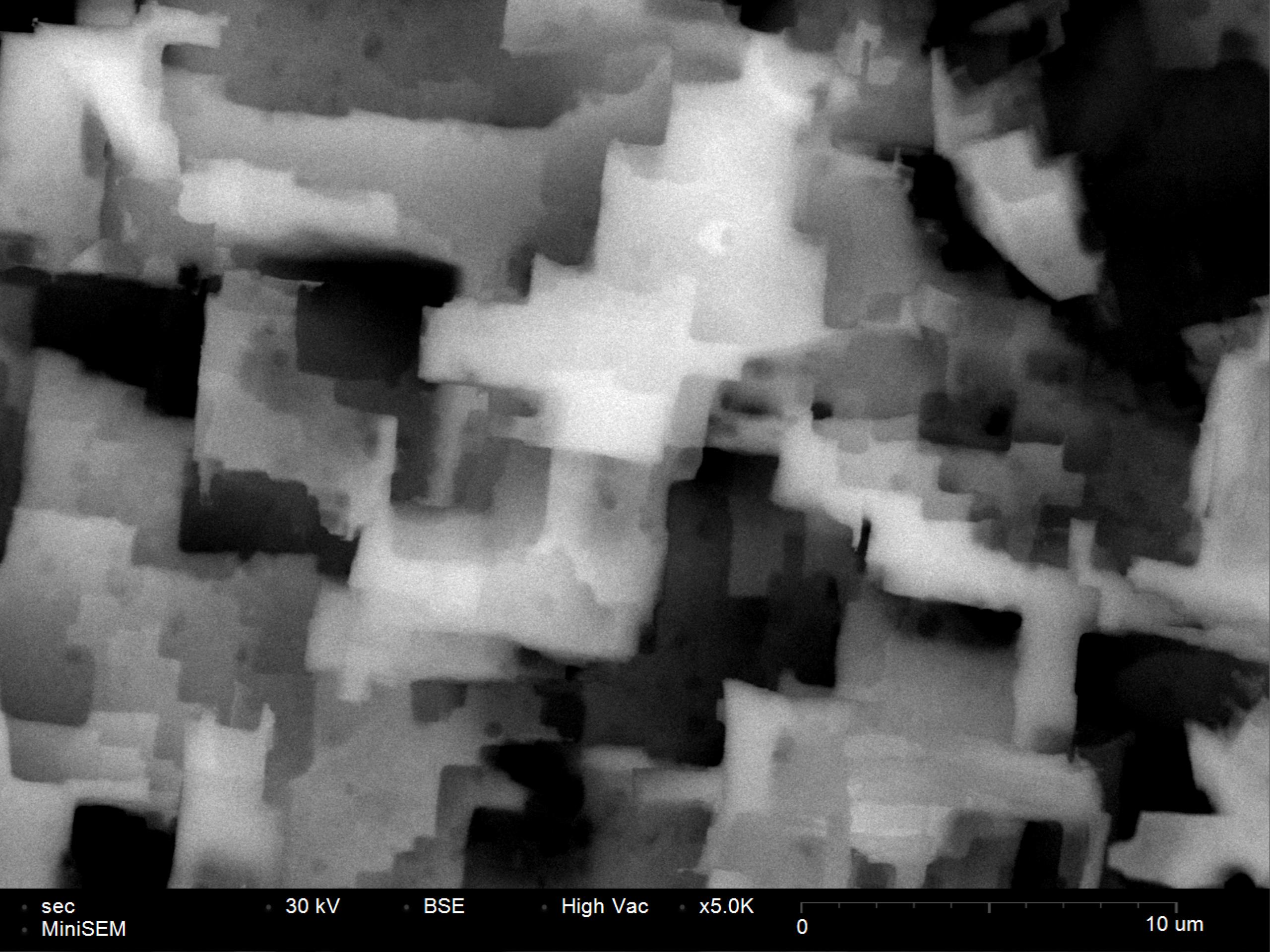
Scanning Electron Microscopy is a non-destructive technique that scans a sample with a focused electron beam and gets images with information about the samples morphology, topography and composition down to nano-scale.
Scanning Electron Microscopes (SEMs) produce high magnification images with high resolution, a feature which makes them an indispensable tool for a wide range of applications in numerous fields of sciences and industry.
SEM produces an image of a sample by scanning the surface of the sample with a highly focused beam of electrons which interact with the sample and produce various signals. These signals are then detected and processed to give surface morphology, topography, and composition of the samples.
